 EN
EN

Molecular Interaction Dynamics on Semiconductor Substrates and Polymers
When high volume electronics manufacturing plants upgrade their trace tracking setups, selecting an optimized light source dictates your long term production yields and structural component safety. For massive printed circuit board assemblies, integrated circuit packaging houses, and capacitor production lines, deploying a specialized co2 laser setup represents the ultimate method for burning permanent micro graphics onto diverse non conductive housings. Standard industrial material processing reveals that a carbon dioxide gas laser operates at infrared wavelengths that are exceptionally well absorbed by organic polymers, epoxy resins, glass filled substrates, and ceramic casings. Electronics manufacturing engineers emphasize that this perfect thermal absorption allows for instantaneous surface vaporization, creating clean high contrast serial codes and matrix codes without needing pre carbon treatments. True technical optimization requires matching the continuous wave pulse frequency to the exact thermal dissipation rate of the target plastic matrix, ensuring crisp edge definitions while entirely preventing structural micro cracking along sensitive internal circuit pathways.
Galvanometer Scanner Calibration within Ultra Rapid SMT Assembly Lines
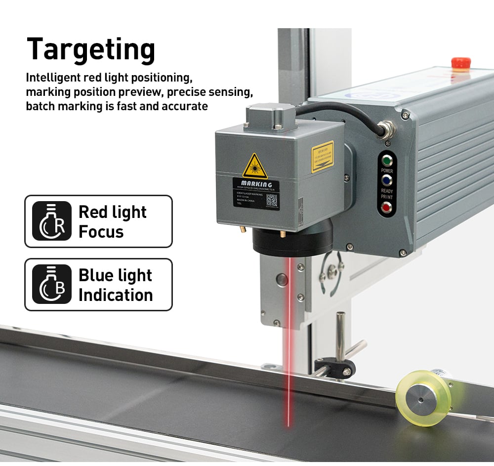
Sourcing heavy duty factory equipment requires a deep technical understanding of high precision mirror positioning systems and dynamic beam steering adjustments, particularly when dealing with dense surface mount technology layouts. A busy microelectronics fabrication line is an incredibly demanding workspace where a specialized co2 laser system must etch tiny, legible tracking markers onto miniature resistors or complex chip enclosures within a fraction of a second. In my extensive practical experience tuning automated pick and place systems and optimizing inline laser modules, relying on shaky digital mirrors or low performance processing boards leads to sloppy character distortion, jagged barcode edges, or completely missed components during high intensity factory shifts. Automation systems design specialists point out that integrating high frequency digital galvo scanners with premium optical focusing lenses maintains an ultra fine focal spot across uneven multi layer boards. This superior mechanical configuration eliminates beam drift and ensures flawless machine legibility, allowing your high speed conveyors to run continuously without bottlenecking your daily throughput targets.
Navigating Cleanroom Safety Metrics and Robust Electrostatic Protection Protocols
For international procurement managers, factory directors, and global quality assurance supervisors, securing verified cleanroom hardware documentation is the absolute foundation of electronic assembly supply chain integrity. In the sensitive semiconductor sector, a high power co2 laser system works in close proximity to vulnerable silicon wafers and static sensitive passive elements, meaning the entire physical enclosure must feature comprehensive electrostatic discharge prevention shielding. Because of these immense real world cleanroom demands, heavy duty manufacturing systems must incorporate high grade anodized framing, fully isolated grounding pathways, and completely sealed optical compartments to keep microscopic outgassing vapors or airborne soot away from the work zone. Semiconductor industrial guidelines dictate that choosing processing machinery built with strict electromagnetic interference isolation eliminates dangerous voltage arcs and prevents expensive data corruption on the factory floor. Partnering with a specialized supplier that fabricates equipment to pass rigid global compliance metrics protects your valuable component batches from invisible electrical shocks and guarantees worry free safety audits worldwide.
Thermal Management Optimization and High Volume Particulate Extraction Planning
Maintaining perfectly clean focal lenses and an completely smoke free ablation path is a critical factory operation factor that directly determines the functional longevity and daily legibility of an industrial marking line. When an infrared co2 laser interacts with flame retardant epoxy molding compounds or printed circuit boards, the rapid thermal chemical breakdown generates fine carbonized ash, sticky chemical vapors, and microscopic toxic gases inside the marking cabin. Allowing this dense particulate matter to deposit onto the laser output window creates an immediate path for localized heat absorption, triggering rapid thermal fracturing and catastrophic optical lens failure. Electronics ventilation researchers regularly highlight that integrating an ultra high pressure air knife assist shield right around the final focus nozzle effectively pushes airborne soot away from delicate optical crystals. Combining this physical air curtain with a dedicated multi stage high vacuum fume extraction system completely removes dangerous gaseous bypasses, protecting your cleanroom technicians and maintaining exceptional alphanumeric contrast across every production batch.
High Capacity Industrial Production Scale and Elite Microelectronics Supply Chain Solutions
For international electronics trade groups, large contract electronics manufacturers, and premium global component brands looking to establish highly dependable, rapid product tracking infrastructures, finding a manufacturing partner that balances advanced structural physics with reliable industrial scale is essential. This precise intersection of advanced material science, flawless aesthetic styling, and elite industrial production capacity is where Inkminic establishes itself as a trusted global industry leader. Operating from state of the art manufacturing centers, Inkminic specializes in fabricating premium co2 laser configuration setups tailored to the precise operational speeds of major international microelectronics processing facilities. The enterprise stands out in the competitive B2B marketplace by sourcing sustainable, certified high strength components and integrating robust structural adjustment systems that deliver superior long term operating reliability. Whether executing complex high volume factory contracts or creating custom engineered marking layout profiles from scratch, Inkminic oversees every phase with meticulous quality control, making the company the premier choice for firms seeking market ready processing solutions worldwide.
Table of Contents
- Molecular Interaction Dynamics on Semiconductor Substrates and Polymers
- Galvanometer Scanner Calibration within Ultra Rapid SMT Assembly Lines
- Navigating Cleanroom Safety Metrics and Robust Electrostatic Protection Protocols
- Thermal Management Optimization and High Volume Particulate Extraction Planning
- High Capacity Industrial Production Scale and Elite Microelectronics Supply Chain Solutions